Semiconductor Equipment

Semiconductor Equipment

Semiconductor Equipment
APPLICATION SOLUTION

Semiconductor Equipment

Semiconductor equipment is the core precision machinery for integrated circuit manufacturing. Metal 3D printing enables integrated forming of complex structures, balancing lightweight, high stiffness, low vibration and efficient thermal management to improve the dynamic performance, positioning accuracy and temperature stability of wafer stages. It also increases material utilization, reduces welding, assembly and machining steps, and lowers manufacturing costs and post-processing requirements such as cleaning.

Discuss Your Application →
TYPICAL APPLICATION CASES

Typical Application Cases

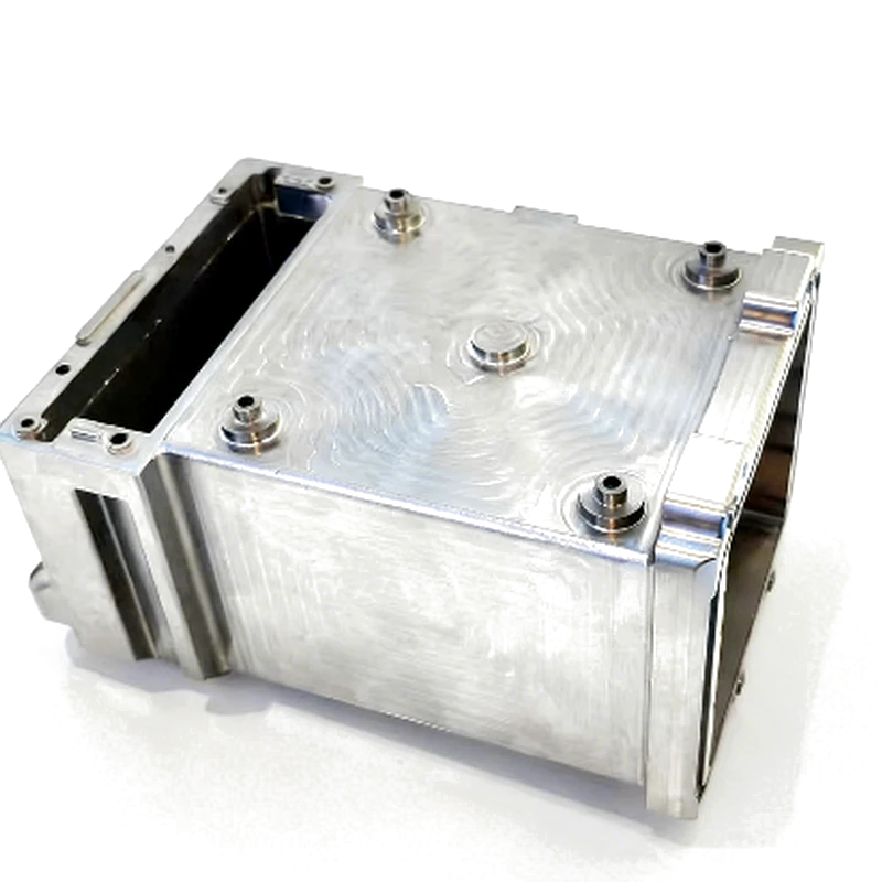
Water Cooling Box

Water Cooling Box

Material:
TC4
Size:
159×109×84(mm)
Usage:
Temperature control for etching, deposition, ion implantation and other semiconductor equipment

Structural Features:TC4 titanium alloy integrated printing, built-in composite channels, weld-free high sealing, ±0.1 °C precision temperature control, corrosion-resistant and low contamination, long life and high reliability.
Water Cooling Manifold

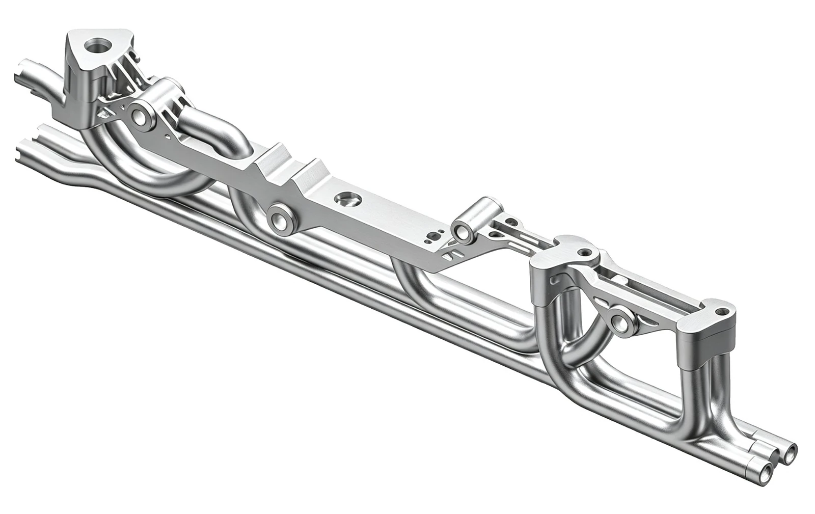
Water Cooling Manifold

Material:
TC4
Size:
53×23×255(mm)
Usage:
Provides centralized fluid distribution and delivery for multi-spec water cooling boxes / chambers

Structural Features:TC4 integrated printing, multi-outlet distribution channels, precise flow distribution, suitable for centralized semiconductor fluid supply, no solder joints or leaks, even flow distribution, low pressure drop, corrosion-resistant and low outgassing, high reliability.

Showerhead

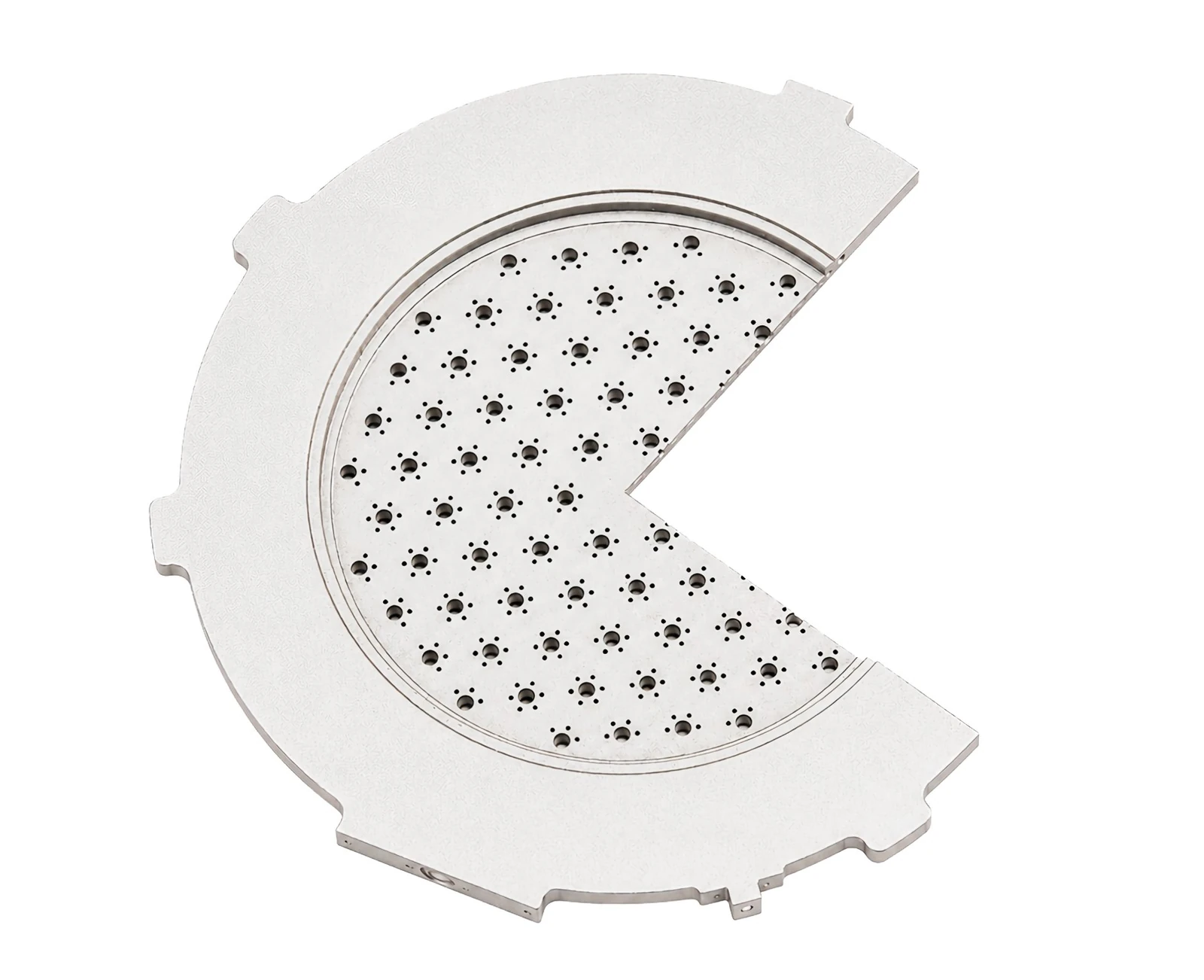
Showerhead

Material:
TC4
Size:
370×370×23(mm)
Usage:
Precise and uniform distribution of process gases for etching and deposition

Structural Features:C-shaped structure densely populated with 0.4 mm micro-holes, integrated mounting and positioning; excellent gas-flow uniformity, corrosion-resistant and low outgassing, improves wafer process yield.

Wafer Chuck

Wafer Chuck

Material:
AlSi10Mg
Size:
310×310×52(mm)
Usage:
Suitable for precision wafer clamping in lithography, etching, deposition

Structural Features:Integrated forming, built-in vacuum channels, lightweight precision wafer clamping, mirror-grade flatness reference; stable clamping without deformation, flatness < 2 μm, excellent thermal uniformity.